forwarded clock command
create_generated_clock -name Clkout -source [get_pins ODDR_inst/C] -combinational [get_pins ODDR_inst/Q]
forwarded clock command
create_generated_clock -name Clkout -source [get_pins ODDR_inst/C] -combinational [get_pins ODDR_inst/Q]
This finds all the cells of a certain type but it doesn’t check if the CE is connected to VCC
show_objects -name find_1 [get_cells -hierarchical -filter { PRIMITIVE_TYPE == REGISTER.SDR.FDCE } ]
This however is more through: finds all flops with an enable pin and then verifies that it’s not connected to power (vcc)
set ffs_with_ce {}
foreach ff [get_cells -hier -filter {PRIMITIVE_SUBGROUP == “flop”}] {
if {[get_property TYPE [get_nets -of_objects [get_pins -of_objects $ff -filter IS_ENABLE]]] != “POWER”} {lappend ffs_with_ce $ff}
}
In recent generations of Xilinx FPGAs a new feature has been introduced: HARD_SYNC dedicated synchronization registers.
These are hardwired/dedicated blocks with 3 registers specifically designed with synchronization purposes.
It’s possible to configure a hard_sync synchronizer for 2 or 3 stages of shift registers. These should give the best defence against meta-stability while sampling asynchronous signals.
Here is how they are used in Verilog:
HARD_SYNC #(
.INIT(1’b0), // Initial value
.IS_CLK_INVERTED(1’b0), // configurable inverted clock
.LATENCY(2) // 2-3 stage shift register
)
uhardsync (
.DIN(DIN), // input Data
.DOUT(DOUT), // output Data
.CLK(CLK) // Clock
);
(* ALLOW_COMBINATORIAL_LOOPS = “true”, KEEP = “true” *) wire ring;
In Vivado, one way to cleanup timing after final place & route is to unplace the cells in the worst negative slack path and just place & route that portion. I have had great success with this in the GUI flow. It’s quite easy there. You just do a timing report (report_timing_summary), right-click on the timing path and say unplace cells. Then you run the cleanup commands.
Of course it’s tedious to do this manually but one has to find all the cells involved in a timing path. Here is what I came up with:
set string [report_timing -no_header -path_type full -return_string]

set items [split string]

foreach item $items {if [regexp {TOP\/.*$} item] {lappend cells [get_cells -filter {IS_PRIMITIVE==1} -of_objects [get_pins $item]]))
So here we get a timing report, find all fields in it then if the item starts with our TOP module name, we assume it’s a pin name and get the cell of that pin. This finds some of the same cells twice but unplacing an already unplaced cell is fine so we don’t have to worry about duplicates.
Finally one can do
unplace_cell $cells

place_design -directive Explore

route_design -directive Explore

route_design -tns_cleanup

phys_opt_design -directive Explore
for final rip & re-route stage. I usually get very good timing results from this.
set_property -name {xsim.simulate.runtime} -value {9000ns} -objects [get_filesets sim_1]
set_param synth.elaboration.rodinMoreOptions {rt::set_parameter minFsmStates 4}
AR #65413 is a really annoying answer record from Xilinx. They are basically saying that a perfectly legitimate piece of code won’t work in Vivado synthesis and they have no intention of fixing it. Alas the following code will not work:
generate

  for (g=0; g < D; g++) begin: regs

    //string rlocval;

    //localparam string rlocpre = "X0Y";

    //localparam string rloc = {rlocpre, rlocval.itoa(g/8)};

    localparam rlocpre = "X0Y";

    localparam byte rlocbyte = g/8 + 48;

    localparam rloc = {rlocpre, rlocbyte};

    localparam bel[8] = {"AFF", "A5FF", "BFF", "B5FF", "CFF", "C5FF", "DFF", "D5FF"};

    (* RLOC = rloc, BEL = bel[g%8] *) FDRE u(.C(clk), .D(d[g]), .Q(q[g]), .CE(1'b1), .R(1'b0));

  end

endgenerate
Omnivision Image sensors support a serial control interface called SCCB Omnivision SCCB spec
The main difference between SCCB & I2C is that it’s specified as SCLK being output only and active driver instead of open-drain (or tri-state or open-collector). If one actually wants to remove the pull-up on the SCLK and use this feature, it causes a minor issue with some I2C IP blocks in FPGA as they assume open-drain SCLK. Specifically in Xilinx AXI IIC controller, the IP generates 3 signals (scl_i, scl_o, scl_t) which are normally used to control a set of IBUF & OBUFT pads to drive scl_io PAD. The way to use this IP in an SCCB setting is to use the scl_t signal to drive the scl_io. Xilinx OBUFT has an active high tri-state so scl_t is high when scl_io needs to be pulled-up and it’s low with scl_o being also low. So scl_t carries the intent of scl_io signal when active driven. Also scl_i should be connected to scl_t for the IP to sense the driven signal.
One final complication is that if one makes the IIC interface external and uses some of the signals in the Vivado block diagram, Vivado makes all remaining signals external too which creates non-existing pins so all scl_x signals (other than scl_t) should be consumed inside the block diagram. scl_i being connected to scl_t takes care of that signal but scl_o should also be consumed. One can use it as an active low source or “or” it to another signal (it’s always zero so it can’t hurt) for it to be not exported out of the top level wrapper.
ERROR: [Synth 8-4556] size of variable … is too large to handle
set_param synth.elaboration.rodinMoreOptions “rt::set_parameter var_size_limit 4194304”
use the above switch to increase the variable size limit.
set_param synth.elaboration.rodinMoreOptions {rt::set_parameter dissolveMemorySizeLimit 147456}
this is for Synth 8-3391 Error.
set_param synth.elaboration.rodinMoreOptions “rt::set_parameter supportAsymRam true”
This is probably fixed. Asymmetric read/write width support.
set_param synth.elaboration.rodinMoreOptions “rt::set_parameter compatibilityMode true”
set_param synth.elaboration.rodinMoreOptions “rt::set_parameter controlSetsOptMaxFlops 10000”
setting controlSetsOptMaxFlops to 10000 will further allow optimizations on control sets into registers.
set_param synth.elaboration.rodinMoreOptions {rt::set_parameter simplifyCascadedMerge 0;rt::set_parameter mergeReconvergentCasePartitions false; rt::set_parameter mergeReconvergentLogicPartitions false}
Helps with how the Vivado Synthesis compiler is unrolling loops.
set_param synth.elaboration.rodinMoreOptions “rt::set_parameter reduceVariableBitSelect false; rt::set_parameter reinferPruneBitWidths false; rt::set_parameter constPropCarry false”
set_param synth.elaboration.rodinMoreOptions “rt::set_parameter forcePackBramAddrReg true”
the address register is not pulled into the block RAM if it has a feedback structure so this workaround is needed.
set_param synth.elaboration.rodinMoreOptions “rt::set_parameter doBramAddrRegResetTransform true”
This will pull reset from the address register so that it can be used to infer BRAM.
set_param synth.elaboration.rodinMoreOptions “rt::set_parameter constPropCarry false”
This problem is due to an optimization of constant logic during synthesis. Probably fixed in 2014.3
Vivado implementation tools are really getting close to their ASIC counterparts in terms of capability. The command phys_opt_design now implements useful skew insertion to meet timing. Useful skew is a technique where clock tree is manipulated to have non-zero skew for pipelines which are not completely balanced. Imagine 3 registers, R1, R2, R3 and 2 combinational blocks between them D1 and D2 between R1, R2 and R2, R3 respectively. Now if the delay of D1 block is longer than D2 and this causes timing failures, one has several options to remedy this situation. One can change the RTL and try to balance D1 and D2. This is the least desirable solution as it forces one to run all the regression tests again because RTL is modified. The second solution is to apply register retiming during implementation, ie let the physical optimization tool move some of the logic from D1 to D2 at mapped, maybe even placed gate level. This has a lower cost than RTL changes but it complicates formal verification efforts because now the RTL pipeline does not match gate level pipeline and formal verification needs to understand what retiming has been done. Also one has to verify that no sequential behavior has been changed.
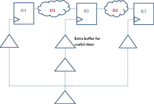
The third and the lowest cost option is to add useful skew to the design. This is accomplished by increasing the time available to D1 block and reducing the time available to D2 block by adjusting the clock tree. Usually clock trees are designed for zero-skew ie all registers in a clock domain see a clock edge as close to each other as possible ie all leaf nodes of a clock tree to each register have the same delay from the root. This facilitates hold timing correctness and flops usually have a output delay larger than hold requirement so with zero-skew even a shift register with no delay between the two registers is guaranteed to have no hold violations with zero-skew. Useful skew changes this design paradigm. In our example because D1 is longer than D2, when it misses timing, there might be positive slack in the D2 path. In this case if we increase the skew to R2 register, this will make more time available to D1 path and less time available to D2 path. If D2 path has enough positive slack, this will allow both paths to meet timing. This method is the least costly as it is implemented in a post-place, post-route design by the tools and it doesn’t need any change in RTL or logic changes after synthesis and keeps the formal verification flow simple.